Description.
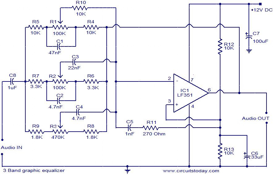
Here is the circuit diagram of a simple 3 band graphic equalizer circuit using a single IC and few components. The IC used here is LF 351 which is a wide bandwidth single JFET operational amplifier. The high input impedance of the IC makes this circuit compatible with most of the audio signal sources. The opamp is wired as an inverting amplifier. The input signal is fed to the inverting input of the opamp via the filter network. The filter network can produce a +/- 20 dB enhancement or cut on the three frequency bands 50Hz,1KHz and 10KHz.POTs R1, R2 and R3 can be used for adjusting the gain of the different bands.
Circuit diagram with Parts list.
Notes.
- Assemble the circuit on a general purpose PCB.
- The Circuit can be powered from anything between 6 to 30V DC.
- I am using 12V here.
- Increasing supply voltage will of course increase the gain.
- The IC must be mounted on a holder.
- The electrolytic capacitors must be rated higher than the supply voltage.


16 Comments
Is this for stereo or mono, and does this circuit have full band kill?
Only single channel is shown duplicate for other channel. This is a proven application circuit.
I connected as per the circuit diagram but its not working what audio jack we need to use
Hello can someone give me more information about this circuit?
What level of noise?
What about sound quality?
What sort of pots are required for this, linear or log?
Use LINEAR slider POTS as the circuit is an active feedback Baxandall Tone control. R1 is BASS control, R2 is MID FREQ Control and R3 is TREBLE Control. If all the controls are set center position the gain is approx unity, input and out put will be same no attenuation.
Can you give dual supply 3 band equaliser ckt with volume contro details?
I am saticefied veery well.Also pls improve this site from newly discovered circuits.