LCD display is an inevitable part in almost all embedded projects and this article is about interfacing a 16×2 LCD with 8051 microcontroller. Many guys find it hard to interface LCD module with the 8051 but the fact is that if you learn it properly, its a very easy job and by knowing it you can easily design embedded projects like digital voltmeter / ammeter, digital clock, home automation displays, status indicator display, digital code locks, digital speedometer/ odometer, display for music players etc etc. Thoroughly going through this article will make you able to display any text (including the extended characters) on any part of the 16×2 display screen. In order to understand the interfacing first you have to know about the 16×2 LCD module.
16×2 LCD module.
16×2 LCD module is a very common type of LCD module that is used in 8051 based embedded projects. It consists of 16 rows and 2 columns of 5×7 or 5×8 LCD dot matrices. The module were are talking about here is type number JHD162A which is a very popular one . It is available in a 16 pin package with back light ,contrast adjustment function and each dot matrix has 5×8 dot resolution. The pin numbers, their name and corresponding functions are shown in the table below.
| Pin No: | Name | Function |
| 1 | VSS | This pin must be connected to the ground |
| 2 | VCC | Positive supply voltage pin (5V DC) |
| 3 | VEE | Contrast adjustment |
| 4 | RS | Register selection |
| 5 | R/W | Read or write |
| 6 | E | Enable |
| 7 | DB0 | Data |
| 8 | DB1 | Data |
| 9 | DB2 | Data |
| 10 | DB3 | Data |
| 11 | DB4 | Data |
| 12 | DB5 | Data |
| 13 | DB6 | Data |
| 14 | DB7 | Data |
| 15 | LED+ | Back light LED+ |
| 16 | LED- | Back light LED- |
VEE pin is meant for adjusting the contrast of the LCD display and the contrast can be adjusted by varying the voltage at this pin. This is done by connecting one end of a POT to the Vcc (5V), other end to the Ground and connecting the center terminal (wiper) of of the POT to the VEE pin. See the circuit diagram for better understanding.
The JHD162A has two built in registers namely data register and command register. Data register is for placing the data to be displayed , and the command register is to place the commands. The 16×2 LCD module has a set of commands each meant for doing a particular job with the display. We will discuss in detail about the commands later. High logic at the RS pin will select the data register and Low logic at the RS pin will select the command register. If we make the RS pin high and the put a data in the 8 bit data line (DB0 to DB7) , the LCD module will recognize it as a data to be displayed . If we make RS pin low and put a data on the data line, the module will recognize it as a command.
R/W pin is meant for selecting between read and write modes. High level at this pin enables read mode and low level at this pin enables write mode.
E pin is for enabling the module. A high to low transition at this pin will enable the module.
DB0 to DB7 are the data pins. The data to be displayed and the command instructions are placed on these pins.
LED+ is the anode of the back light LED and this pin must be connected to Vcc through a suitable series current limiting resistor. LED- is the cathode of the back light LED and this pin must be connected to ground.
16×2 LCD module commands.
16×2 LCD module has a set of preset command instructions. Each command will make the module to do a particular task. The commonly used commands and their function are given in the table below.
| Command | Function |
| 0F | LCD ON, Cursor ON, Cursor blinking ON |
| 01 | Clear screen |
| 02 | Return home |
| 04 | Decrement cursor |
| 06 | Increment cursor |
| 0E | Display ON ,Cursor blinking OFF |
| 80 | Force cursor to the beginning of 1st line |
| C0 | Force cursor to the beginning of 2nd line |
| 38 | Use 2 lines and 5×7 matrix |
| 83 | Cursor line 1 position 3 |
| 3C | Activate second line |
| 08 | Display OFF, Cursor OFF |
| C1 | Jump to second line, position1 |
| OC | Display ON, Cursor OFF |
| C1 | Jump to second line, position1 |
| C2 | Jump to second line, position2 |
LCD initialization.
The steps that has to be done for initializing the LCD display is given below and these steps are common for almost all applications.
- Send 38H to the 8 bit data line for initialization
- Send 0FH for making LCD ON, cursor ON and cursor blinking ON.
- Send 06H for incrementing cursor position.
- Send 01H for clearing the display and return the cursor.
Sending data to the LCD.
The steps for sending data to the LCD module is given below. I have already said that the LCD module has pins namely RS, R/W and E. It is the logic state of these pins that make the module to determine whether a given data input is a command or data to be displayed.
- Make R/W low.
- Make RS=0 if data byte is a command and make RS=1 if the data byte is a data to be displayed.
- Place data byte on the data register.
- Pulse E from high to low.
- Repeat above steps for sending another data.
Circuit diagram.

The circuit diagram given above shows how to interface a 16×2 LCD module with AT89S1 microcontroller. Capacitor C3, resistor R3 and push button switch S1 forms the reset circuitry. Ceramic capacitors C1,C2 and crystal X1 is related to the clock circuitry which produces the system clock frequency. P1.0 to P1.7 pins of the microcontroller is connected to the DB0 to DB7 pins of the module respectively and through this route the data goes to the LCD module. P3.3, P3.4 and P3.5 are connected to the E, R/W, RS pins of the microcontroller and through this route the control signals are transffered to the LCD module. Resistor R1 limits the current through the back light LED and so do the back light intensity. POT R2 is used for adjusting the contrast of the display. Program for interfacing LCD to 8051 microcontroller is shown below.
Program.
MOV A,#38H // Use 2 lines and 5x7 matrix
ACALL CMND
MOV A,#0FH // LCD ON, cursor ON, cursor blinking ON
ACALL CMND
MOV A,#01H //Clear screen
ACALL CMND
MOV A,#06H //Increment cursor
ACALL CMND
MOV A,#82H //Cursor line one , position 2
ACALL CMND
MOV A,#3CH //Activate second line
ACALL CMND
MOV A,#49D
ACALL DISP
MOV A,#54D
ACALL DISP
MOV A,#88D
ACALL DISP
MOV A,#50D
ACALL DISP
MOV A,#32D
ACALL DISP
MOV A,#76D
ACALL DISP
MOV A,#67D
ACALL DISP
MOV A,#68D
ACALL DISP

MOV A,#0C1H //Jump to second line, position 1
ACALL CMND

MOV A,#67D
ACALL DISP
MOV A,#73D
ACALL DISP
MOV A,#82D
ACALL DISP
MOV A,#67D
ACALL DISP
MOV A,#85D
ACALL DISP
MOV A,#73D
ACALL DISP
MOV A,#84D
ACALL DISP
MOV A,#83D
ACALL DISP
MOV A,#84D
ACALL DISP
MOV A,#79D
ACALL DISP
MOV A,#68D
ACALL DISP
MOV A,#65D
ACALL DISP
MOV A,#89D
ACALL DISP

HERE: SJMP HERE

CMND: MOV P1,A
CLR P3.5
CLR P3.4
SETB P3.3
CLR P3.3
ACALL DELY
RET

DISP:MOV P1,A
SETB P3.5
CLR P3.4
SETB P3.3
CLR P3.3
ACALL DELY
RET

DELY: CLR P3.3
CLR P3.5
SETB P3.4
MOV P1,#0FFh
SETB P3.3
MOV A,P1
JB ACC.7,DELY

CLR P3.3
CLR P3.4
RET

END
Subroutine CMND sets the logic of the RS, R/W, E pins of the LCD module so that the module recognizes the input data ( given to DB0 to DB7) as a command.
Subroutine DISP sets the logic of the RS, R/W, E pins of the module so that the module recognizes the input data as a data to be displayed .
Interfacing LCD Module to 8051 in 4 Bit Mode (using only 4 pins of a port)
The microcontroller like 8051 has only limited number of GPIO pins (GPIO – general purpose input output). So to design complex projects we need sufficient number of I/O pins . An LCD module can be interfaced with a microcontroller either in 8 bit mode (as seen above) or in 4 bit mode. 8 bit mode is the conventional mode which uses 8 data lines and RS, R/W, E pins for functioning. However 4 bit mode uses only 4 data lines along with the control pins. This will saves the number of GPIO pins needed for other purpose.
Objectives
- Interface an LCD with 8051 in 4 bit mode
- Use a single port of the microcontroller for both data and control lines of the LCD.
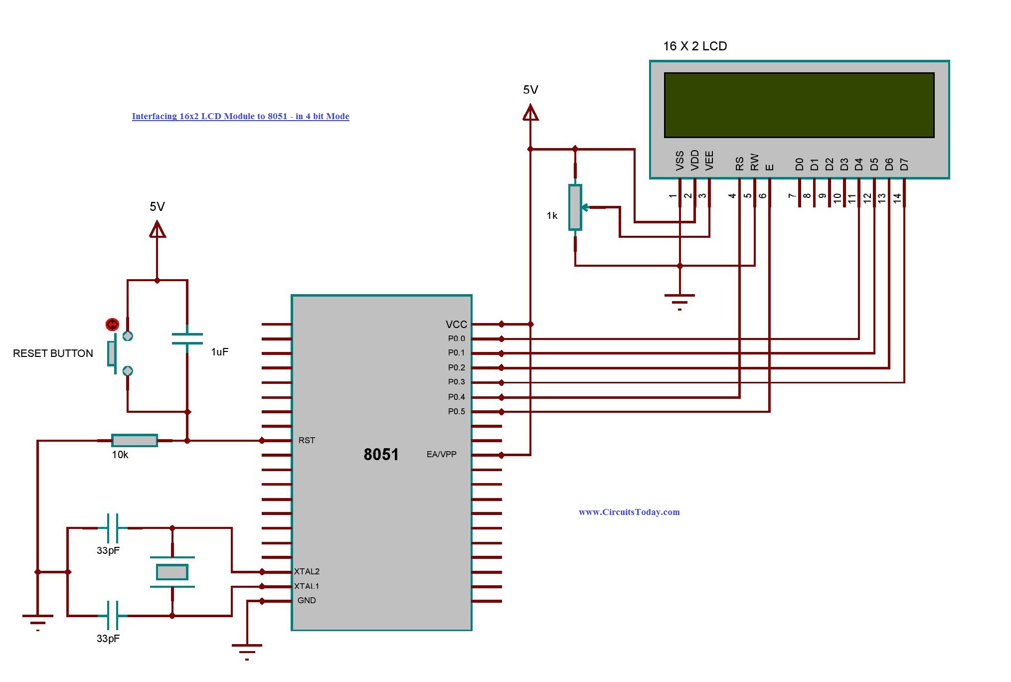
As shown in the circuit diagram, port 0 of the controller is used for interfacing it with LCD module. In 4 bit mode only 4 lines D4-D7, along with RS, R/W and E pins are used. This will save us 4 pins of our controller which we might employ it for other purpose. Here we only need to write to the LCD module. So the R/W pin can be ground it as shown in the schematic diagram. In this way the total number of pins can be reduced to 6. In 4 Bit mode the data bytes are split into two four bits and are transferred in the form of a nibble. The data transmission to a LCD is performed by assigning logic states to the control pins RS and E. The reset circuit, oscillator circuit and power supply need to be provided for the proper working of the circuit.
Program – Interface LCD Module to 8051 – 4 Bit Mode
RS EQU P0.4
EN EQU P0.5
PORT EQU P0
U EQU 30H
L EQU 31H
ORG 000H

MOV DPTR,#INIT_COMMANDS
ACALL LCD_CMD
MOV DPTR,#LINE1
ACALL LCD_CMD
MOV DPTR,#TEXT1
ACALL LCD_DISP
MOV DPTR,#LINE2
ACALL LCD_CMD
MOV DPTR,#TEXT2
ACALL LCD_DISP
SJMP $


SPLITER: MOV L,A
ANL L,#00FH
SWAP A
ANL A,#00FH
MOV U,A
RET

MOVE: ANL PORT,#0F0H
ORL PORT,A
SETB EN
ACALL DELAY
CLR EN
ACALL DELAY
RET


LCD_CMD: CLR A
MOVC A,@A+DPTR
JZ EXIT2
INC DPTR
CLR RS
ACALL SPLITER
MOV A,U
ACALL MOVE
MOV A,L
ACALL MOVE
SJMP LCD_CMD
EXIT2: RET


LCD_DATA: SETB RS
ACALL SPLITER
MOV A,U
ACALL MOVE
MOV A,L
ACALL MOVE
RET

LCD_DISP: CLR A
MOVC A,@A+DPTR
JZ EXIT1
INC DPTR
ACALL LCD_DATA
SJMP LCD_DISP
EXIT1: RET


DELAY: MOV R7, #10H
L2: MOV R6,#0FH
L1: DJNZ R6, L1
DJNZ R7, L2
RET

INIT_COMMANDS: DB 20H,28H,0CH,01H,06H,80H,0
LINE1: DB 01H,06H,06H,80H,0
LINE2: DB 0C0H,0
CLEAR: DB 01H,0

TEXT1: DB " CircuitsToday ",0
TEXT2: DB "4bit Using 1Port",0

END
Important aspects of the program
The programming part is done in assembly language instead of embedded C. As mentioned earlier the 8 bit data is break into two 4 bit data and send to LCD. A subroutine called “SPLITTER” is used in the program for slicing 8 bit data into nibbles. It uses two memory location ‘U’ and ‘L’ for storing the upper and lower nibbles. The subroutine named “MOVE” is used to put the upper and lower nibbles into the data pins of the LCD by making a high to low pulse at the E pin of the LCD module. If we need to send a command, “LCD_CMD” is used. In this subroutine the RS pin of the LCD is cleared in order to notify the LCD that the byte at its data pin is a command. And subroutine labeled “LCD_DISP” is used for sending data. Here the RS pin is set which will notify the LCD that the byte arrived is a data for displaying. The necessary commands for the LCD initialization are defined at the end part of the program. Along with that the text to be displayed is also defined there with a label “TEXT1”. “LINE1” AND “LINE2” labels contains the commands for selecting the 1st and 2nd rows of the LCD respectively.
49 Comments
How to program using loops to display
WE ARE READY
El retardo es demasiado corto
pls provide me program in c program for lcd display to interface with 8051
Good Explanation
is it possible to interface two LCD’s with single 8051 using same control & data pins?
is it possible to interface two LCD’s with 8051 using same pins for control and data?
i have made a pass door lock but when i write the correct pass 12345 it shows wrong pass 🙁 help me reply soon
Please check – https://www.circuitstoday.com/digital-door-lock-password-based-security-8051
16 columns and 2 rows
outstanding…work…
I AM SUPPOSED TO Display MY name on the first line, beginning on the third space. Then display MY city of birth on the second line so that the last character is in the last position
HELP PLZ
ORG 0H
MOV P1,#38H
CLR P1.0
CLR P1.1
SETB P1.2
DELAY: MOV R3,#200
SUE: MOV R4,#255
BOB: DJNZ R4,BOB
DJNZ R3,SUE
CLR P2.2
COMMAND: CLR P2.0
CLR P2.1
SETB P2.2
ACALL DELAY
CLR P1.2
RET
MOV P1,#38H
ACALL COMMAND
MOV A,#0FH
ACALL COMMAND
MOV A,#01H
ACALL COMMAND
MOV A,#06H
ACALL COMMAND
MOV A,#82H
ACALL COMMAND
MOV A,#3CH
ACALL COMMAND
CHECK: SETB P1.7
CLR P1.0
SETB P1.1
JIM: CLR P1.2
ACALL DELAY
SETB P1.2
JB P1.7,JIM
RET
CHAR: SETB P2.0
CLR P2.1
SETB P2.2
ACALL DELAY
CLR P2.2
RET
ACALL CHECK
MOV P1,#0CH
ACALL COMMAND
ACALL CHECK
MOV P1,#01H
ACALL COMMAND
ACALL CHECK
MOV P1,#82H
ACALL COMMAND
ACALL CHECK
MOV DPTR,#ADAM
JAN:CLR A
MOVC A,@A+DPTR
JZ MAROC
MOV P1,A
ACALL CHAR
ACALL CHECK
INC DPTR
SJMP JAN
MAROC: MOV P1,#0C2H
ACALL COMMAND
ACALL CHECK
MOV DPTR,#MOM
SAHRA: CLR A
MOVC A,@A+DPTR
JZ SAIF
MOV P1,A
ACALL CHAR
ACALL CHECK
INC DPTR
SJMP SAHRA
SAIF:SJMP SAIF
ADAM: DB”LAMIAE”,0
MOM: DB” RABAT”,0
END
pls share the alp for lcd interfacing to 8051
hi……..
anybody can send me programing for interfacing light sensor part number TSL45313cl with micro-controller 8051 to give output at 16x2LCD
thanks in advance………….
explain how to display all English alphabets in lcd interfaced with AT89S51
There is nothing appearing on lcd.Please help!
you need to initialize the lcd first ..
Thankyou for taking the efforts!
It works!
hi nothing is appearing on my lcd, circuit is ok and program is copied from yours.
can anybudy send me program for resistance colour code calculator using microcontroller please send asm program
Could you explain me how DELY subroutine produces the delay?
DELY:
MOV P1,#0FFh
MOV A,P1
JB ACC.7,DELY <——
RET;
I mean, when the condition will be met if the program write a full-ones word at P1 every time?
Sorry for the question.
@ Vivek,
It means, if bit 7 of accumulator is SET (that is 1), then jump to the delay routing labelled DELY. I hope you understood 🙂 Any more doubts ?
what is this “JB ACC.7,DELY”? plz reply soon
If the 7th bit of the accumulator is 1,then it jumps to DELY.Else it executes the next instruction
esta muy completa a informacion!! muchas gracias
hi.
can anybody send me circuit and programming of sms based home appliance control system?
Nice explanation…
#include
#include”delay1sec.h”
#define lcd_dat P1
sbit rs=P3^0;
sbit rw=P3^1;
sbit en=P3^2;
void write_lcd(char);
void cmd_lcd(char);
void disp_lcd(char);
void init_lcd();
void str_lcd(char *s);
void int_lcd(unsigned int);
void float_lcd(float);
void write_lcd(char dat)
{
lcd_dat=dat;
rw=0;
en=1; //for latching one byte info
en=0; //clear for latching next info
delay_ms(2);
}
void cmd_lcd(char cmd)
{
rs=0; //set cmd register
write_lcd(cmd);
}
void disp_lcd(char c)
{
rs=1; //set data register
write_lcd(c);
}
void init_lcd()
{
cmd_lcd(0x02); //return cursor home
cmd_lcd(0x38); //8bit mode of operation
cmd_lcd(0x0e); //display on cur off
cmd_lcd(0x01); //clr DDRAM (display data ram)
cmd_lcd(0x06); //shift cursor right after each character displayed
cmd_lcd(0x80); //begin disp from line 1 pos 0
}
void str_lcd(char *s)
{
while(*s)
disp_lcd(*s++);
}
/*
main()
{
init_lcd();
str_lcd(“******”);
cmd_lcd(0xc0);
str_lcd(“*****”);
while(1);
}
*/
main()
{
unsigned char i;
init_lcd();
for(i=0;i<16;i++)
{
cmd_lcd(0x80+i);
str_lcd("WELCOME");
delay_ms(500);
cmd_lcd(0x01);
cmd_lcd(0x80);
}
}
i want lcd program in asm
Anybody can send me the programing for lcd interfacing with microcontroller and xbee s2
Hi I constructed the circuit exactly as it is on my simulator and just copied the program and nothing is appearing on the LCD
Sir,
please try to think this circuit by IC ULN2003 at the place of transistors.
nice work,but please write the programe in embedded c
nice post
nice work dude 🙂
I think that you have use array in c programming. And one thing you have to use a DPTR, LCALL or SJMP, LJMP command in assembler language
absolutely loved this
Thank you Rowan. Please try it. Comment if you come across any doubts.
Real wonderful work………..
Pls provide alp programs for LCD interfacing