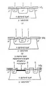
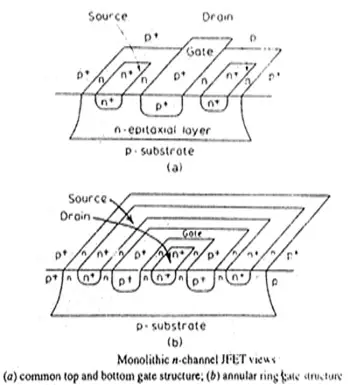
The figure below shows some IC JFET structures. The n-channel JFET structure of first figure [a] is compatible with the n-p-n transistor fabrication sequence. Another view of this n-channel JFET is shown in second figure [a], where we note that the top p+ gate region extends beyond the n-type epitaxial layer region to make contact with the p-type substrate bottom gate. The n-type channel is thus completely encircled by the gate structure and the application of a suitably large negative voltage to the gate can pinch the channel off and reduce the drain-to-source current to essentially zero. If the p+ top gate did not extend out to overlap the p-type substrate, the n-type channel would not be completely encircled by the gate structure and it would not be possible to cut off the drain-to-source current. The major drawback or the JFET structure of second figure [a] is that the gate is connected to the p-type substrate, which is at a ground potential. This restricts the use of this structure to only the common-gate configuration.

Second figure [b] shows another n-channel JFET. Its fabrication is similar to the one just considered, the principal difference being in the top surface geometry. In this JFET the p+ top gate is in the form of an annual ring that completely encloses the drain region of the JFET. The only current path from source to drain will be underneath the p+ top gate. Therefore the application of a suitably large negative voltage to the top gate can pinch off the channel and reduce the drain-to-source current to essentially zero.
First figure [b] shows a p-channel JFET. The n+ gate region of this device extends out beyond the source/drain/channel region to overlap the n-type epitaxial layer so that the gate completely encircles the channel. The same processing sequence can be used for this JFET as for the n-p-n transistor. But, if this is done, the gate-to-channel breakdown voltage (corresponding to BVtRo) will be down in the range 6 to 8V and the full pinch-off of the channel may not be possible. As a result, a specially tailored low-concentration boron diffusion will be required to produce a higher gate –channel breakdown voltage and lower channel doping; so that the channel can be pinched off at a voltage that is conveniently less than the breakdown voltage. This, however, requires some extra processing steps making the device more expensive.

A p-channel JFET employing boron- lon-implanted channel is shown in first figure [c]. Since the ion implantation dosage can be very precisely controlled, the JFET parameters, such as Vp and IDss can be closely set to the values desired This JFET uses the same processing steps as the n-p-n transistor, with the addition of a photolithography, boron ion implantation and annealing step.

3 Comments
Hi Harold the simple solution for your application will be, you can use the digital alarm clock with relay out put or digital output and program it for even few years.
please help me,you can cement if there a clarification so that i will explain the concept of that kind of a circuit.
pleas can you give me a circuit that use in two self timer switch to turn on the first timer in a 6 months then after that,it will turn off.and then automatic turn on the second timer.