In this article, we learn about PN junction diode characteristics in detail – like how to bias a PN junction (Forward & Reverse bias methods), behavior of PN junction during forward & reverse bias setups, how to plot the VI characteristics, what is reverse breakdown and many other essential concepts regarding a PN junction diode. So let’s begin.
In chapter 1 – Understanding the PN junction , we have seen how a PN junction is formed from a p-type and n-type semiconductor. We have also learned about diffusion current, depletion region, drift current and barrier potential. If you find these terms foreign, just read the chapter about “understanding the pn junction” once more. Lets just make some questions. What is the use of a PN junction? Why have scientists created a pn junction device? What kind of problem it solves ? Learning anything is really fun when we question it. So these are our questions. Why there exists a pn junction in this world! ?;)
To get an answer to all these questions, lets first try to understand the characteristics of a PN junction. We know a pn junction has a “barrier potential”. Only if we overcome this “barrier potential” by applying an external voltage to the pn junction, we would be able to make it conducting. This simply means, current will pass through the pn junction only if we apply an external voltage higher than the “barrier potential” of pn junction. In chapter 1, we have seen that  net current inside a pn junction is zero. Inorder to understand the behavior of a pn junction we need to make it conducting by applying an external voltage over a range (say from 0 volts 5 or 10 volts ), and then we study how the current passed through the pn junction varies with increasing voltage levels. To apply an external voltage, we usually connect 2 metallic contacts at the two ends of the pn junction (known as terminals); one on the p-side and other on the n-side. A PN junction with two metallic contacts is known as a pn junction diode or a semiconductor diode.Â
Note:- I have written an interesting article which tells the story behind invention & discovery of PN Junction diode. If you like to read the story, follow here:- Story behind Invention & Discovery of PN Junction

PN junction diode is symbolically represented as shown in picture. The direction of arrow is the direction of conventional current flow (under forward bias). Now lets try applying an external voltage to the pn junction diode. The process of applying an external voltage is called as “biasing”. There are two ways in which we can bias a pn junction diode.
1) Forward bias and 2) Reverse biasÂ
The basic difference between a forward bias and reverse bias is in the direction of applying external voltage. The direction of external voltage applied in reverse bias is opposite to that of  external voltage applied in forward bias.
Forward biasing a PN Junction diode

Forward biasing a pn junction diode is very simple. You just need to take a battery whose values can be varied from (o to V volts), connect its positive terminal to the p-side of pn junction diode and then connect the negative terminal of battery to the n-side of the pn junction diode. If you have done upto this, the forward bias circuit of pn junction diode is complete. Now all we need to do is understand how the pn junction diode behaves when we increase the voltage levels from 0 to say 10 volts or 100 volts. We have learned that if we apply an external voltage higher than the barrier potential of pn junction diode, it will start conducting, which means it will start passing current through it. So how we are going to study the behavior of pn junction diode under forward biased condition? Lets get a voltmeter and ammeter and connect it to the forward biased circuit of pn junction diode.A simple circuit diagram is shown below, which has a pn junction diode, a battery (in picture it is not shown as variable. keep in mind we are talking about a variable power source), an ammeter (in milli ampere range) and a voltmeter.

Note:- Assume that the pn junction diode is made from Silicon. The reason is difference in barrier potential for a diode made from Germanium and Silicon. (For a silicon diode – barrier potential is 0.7 volts where as for a Germanium diode barrier potential is low ~ 0.3 volts)
How to plot the characteristics of a pn junction ?
What we are going to do is, vary the voltage across diode by adjusting the battery. We start from o volts, then slowly move 0.1 volts, 0.2 volts and so on till 10 volts. Lets just note the readings  of voltmeter and ammeter each time we adjust the battery (in steps of 0.1 volts). Finally after taking the readings, just plot a graph with voltmeter readings on X-axis and corresponding Ammeter readings on Y axis. Join all the dots in graph paper and you will see a graphical representation as shown below. Now this is what we call “characteristics of a pn junction diode” or the “behavior of diode under forward bias”Â
How to analyse the characteristics of a pn junction diode ?

Its from the “characteristics graph” we have just drawn, we are going to make conclusions about the behavior of pn junction diode. The first thing that we shall be interested in is about “barrier potential”. We talked a lot about barrier potential but did we ever mention its value ? From the graph, we observe that the diode does not conduct at all in the initial stages. From 0 volts to 0.7 volts, we are seeing the ammeter reading as zero! This means the diode has not started conducting current through it. From 0.7 volts and up, the diode start conducting and the current through diode increases linearly with increase in voltage of battery. From this data what you can infer ? The barrier potential of silicon diode is 0.7 volts 😉 Â What else ? The diode starts conducting at 0.7 volts and current through the diode increases linearly with increase in voltage. So that’s the forward bias characteristics of a pn junction diode. It conducts current linearly with increase in voltage applied across the 2 terminals (provided the applied voltage crosses barrier potential).
What happens inside the pn junction diode when we apply forward bias ?
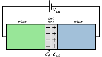
We have seen the characteristics of pn junction diode through its graph. What really happens inside the diode during the forward bias ? We know a diode has a depletion region with a fixed barrier potential. This depletion region has a predefined width, say W. This width will vary for a Silicon diode and a Germanium diode. The width highly depends on the type of semiconductor used to make pn junction, the level of doping etc. When we apply voltage to the terminals of diode, the width of depletion region slowly starts decreasing. The reason for this is, in forward bias we apply voltage in a direction opposite to that of barrier potential. We know the p-side of diode is connected to positive terminal and n-side of diode is connected to negative terminal of battery. So the electrons in n-side gets pushed towards the junction (by force of repulsion) and the holes in p-side gets pushed towards the junction. As the applied voltage increases from 0 volts to 0.7 volts, the depletion region width reduces from ‘W’ to zero. This means depletion region vanishes at 0.7 volts of applied voltage.  This results in increased diffusion of electrons from n-side to p-side region and the increased diffusion of holes from p-side to n-side region. In other words, “minority carrier” injection happens on both p-side (in a normal diode (without bias) electrons are a minority on p-side) and n-side (holes are a minority on n-side) of the diode.
How current flow takes place in a pn junction diode ?
This is another interesting factor, to explain. As the voltage level increases, the electrons from n-side gets pushed towards the p-side junction. Similarly holes from p-side gets pushed towards the n-side junction. Now there arises a concentration gradient between the number of electrons at the p-side junction region and the number of electrons at the region towards the p-side terminal. A similar concentration gradient develops between the number of holes at the n-side junction region and the number of holes at region near the n-side terminal. This results in movement of charge carriers (electrons and holes) from region of higher concentration to region of lower concentration. This movement of charge carriers inside pn junction gives rise to current through the circuit.
Reverse biasing a PN junction diode
Why should we reverse bias a pn diode ? The reason is, we want to learn its characteristics under different circumstances. By reverse biasing, we mean, applying an external voltage which is opposite in direction to forward bias. So here we connect positive terminal of battery to n-side of the diode and negative terminal of the battery to p-side of the diode. This completes the reverse bias circuit for pn junction diode. Now to study its characteristics (change in current with applied voltage), we need to repeat all those steps again. Connect voltmeter, ammeter, vary the battery voltage, note the readings etc etc. Finally we will get a graph as shown.

Analysing the revere bias characteristics
Here the interesting thing to note is that, diode does not conduct with change in applied voltage. The current remains constant at a negligibly small value (in the range of micro amps) for a long range of change in applied voltage. When the voltage is raised above a particular point, say 80 volts, the current suddenly shoots (increases suddenly). This is called as “reverse current” and this particular value of applied voltage, where reverse current through diode increases suddenly is known as “break down voltage“.
What happens inside the diode ?
We connected p-side of diode to negative terminal of battery and n-side of diode to positive terminal of battery. So one thing is clear, we are applying external voltage in the same direction of barrier potential. If applied external voltage is V and barrier potential is Vx , then total voltage across the pn junction will be V+Vx. The electrons at n-side will get pulled from junction region to the terminal region of n-side and similarly the holes at p-side junction will get pulled towards the terminal region of p-side. Â This results in increasing the depletion region width from its initial length, say ‘W’ to some ‘W+x’. As width of depletion region increases, it results in increasing the electric field strength.
How reverse saturation current occurs and why it exists ?
The reverse saturation current is the negligibly small current (in the range of micro amperes) shown in graph, from 0 volts to break down voltage. It remains almost constant (negligible increase do exist) in the range of 0 volts to reverse breakdown voltage. How it occurs ? We know, as electrons and holes are pulled away from junction, they dont get diffused each other across the junction. So the net “diffusion current” is zero! What remains is the drift due to electric field. This reverse saturation current is the result of drifting of charge carriers from the junction region to terminal region. This drift is caused by the electric field generated by depletion region.
What happens at reverse breakdown ?
At breakdown voltage, the current through diode shoots rapidly. Even for a small change in applied voltage, there is a high increase in net current through the diode. For each pn junction diode, there will be a maximum net current that it can withstand. If the reverse current exceeds this maximum rating, the diode will get damaged.
Conclusion about PN junction characteristics
To conclude about pn junction characteristics, we need to get an answer to the first question we have raised – What is the use of pn junction? From the analysis of both forward bias and reverse bias, we can arrive at one fact – a pn junction diode conducts current only in one direction – i.e during forward bias. During forward bias, the diode conducts current with increase in voltage. During reverse bias, the diode does not conduct with increase in voltage (break down usually results in damage of diode). Where can we put this characteristics of diode into use ? Hope you got the answer! Its in conversion of alternating current to direct current (AC to DC). So the practical application of pn junction diode is rectification!
Hey! That’s so helpful
Thickness of diplition layer depend on which factor?
Hello,
DESC: Diode forward biased 24VDC
QTY: 20pcs
DESC: Diode Reverse biased 24VDC
QTY: 20pcs
Regards,
Faith N. Dolorito
Procurement Specialist
MANILA OVERSEAS INC. TEL:6328004227 FAX:6328004172
like this
thank you so very much….
I am clearly understood to read it…….
……..
As width of depletion region increases, it results in increasing the electric field strength.Why?
What is zener effect and avalanche effect.?
Utmost/extremly thanks …..
For this crystal clear explanation…..
I really got something from it….
But sir what is Zener effect.and avalenche effect.?
Why internal electric field generate after diffusion process in pn junction
i hve a question.
why the arrow in pn junction thicker????
explain the working of PN junction diode in forward and reverse biasing configuration please ?
why the battery in reverse bias is greater than in forward bias
I think I missed something. You say that the PN junction only starts to conduct current after the voltage aplied on the diode (Vd) reaches 0.7V, the barrier potential as you call it, but all the graphics and equations shows us that there is current through the diode for values of Vd smaller than 0,7V. I mean, even considering the current for Vd near zero negligible, with Vd~0.60V there is current.
As I see it, we just consider 0.7V as a practival value for a conducting diode, where any variation of the current will cause a small variation on Vd, keeping it around the same 0.7V.
It would me consistent with the diode current equation Id=Is(exp(Vd/nVt)-1), cause in 0.7V for a regular diode, de slope in the curve is too large to see any change in Vd as the current varies.
I don’t know if I made myself clear, but thats a point that is not really clear in many books about semiconductors physics and it’s annoying me. If you could clarify that for me I would be glad.
Why the forward voltage values are almost constant for source voltage from 5V to 1V during forward-biased?
what is the difference between the connections of forwardbias and reverse bias in pn junction…?
in forward biasis -VE terminal of battery is connected to pentavelent group N and +ve is connected to trivalent group P
but in reverse biasis the connection is opposite …
can I get a pdf of this chapter??
no
very clear presantation if you were around i would offer you a cup of tea or coffee good work
why is the voltmeter connected across the ammeter and reverse biased diode..?
Can a diode work on ac voltage or not
@Anuj – A diode is basically a PN Junction. It is used to convert AC to DC.
diode worked on ac voltage but it will give output is DC why because ac has two half cycles in that case,it will conduct only positive half cycle….do not allow -ve cycles…
it’s working on ac voltage
The junction information is clearly understand so nice of it thanx
for eachelectron hole combination that take place near the junction a covalent bond breaks in the p section near the +ve pole of the battery how it is formed?
for eachelectron hole combination that take place near the junction a covalent bond breaks in the p section near the +ve pole of the battery how it is formed?
it is so helpful and it clears all the confusion…….plz answer meone question thatis why in CB mode the emitter current increases with increase of V(CB)
this is a exellent article……….sir plz letme know about base width modulation
It is very short notes
It is very useful
i am very happy after read that notes thank u very much
thanks 4 the good explanation. will you please show the one connected image source circuit of both forward and reverse biased a pn-junction
Please see Fig.10
wow it is very much helpful to me. Thanks the author
yes, its very great answer that i want. Thanks.
I really appreciate. Got a clearer explanation that i did in class… Kudos.
Thanks Admin
a great work with full clearification. thanx !
Really interesting and clear clarification of every aspect of a junction diode characteristics.Very nice
Brilliant! Very helpful article. It’s clearly explaind and easy to understand. Bravo for the person who has put so much work to make it!!
Thanq So Much 🙂 this helped me a lot 🙂 Is there explanation for Transistor as a Switch and Amplifier?
explanation is little bit invalid
thaks very much for the good explanation.can you describe the current voltage characteristics of a photodiode when light is incident on it?
veryyyy goood explanation, i got it perfectly, please tell me about bridge wave rectifier, we connect 4 diodes in bridge but when the d1 and d2 are forward biased then haw the d3 and d4 are reversr biased
@Nayan – Read this article:- https://circuitstoday.com/full-wave-bridge-rectifier
It will help you understand bridge rectifier perfectly.
when we talk about reverse bias ,thn the width of depletion layer increases thn after more reverse voltage(greater than reverse breakdown voltage) how current flow through dide?
@ramdas
At break down, what happens really is that the diode gets damaged. It loses its junction & characteristics associated with the junction. The “diode” almost behaves like a shorted wire & hence current flows through it easily. Theoretically, internal resistance of a diode at breakdown is zero. But in practice, there exists a small internal resistance and hence the current increases with a deviation factor (and not a perpendicular graph).
Hope this helps!
Really helpfull , Thanks sir..
good explanation with neat a diagrams
its very simple to understand ……i like to read a lot in webpage…thank u to author who wrote this.
well explained. really enyoyed.
sir please add the curve charcterstic found when we use ge semiconductor as pn junction diode due to the this experiment
it was very useful and was written in a readble mannar
I like this and I enjoy
its a rely nuc explanation abt pn junctoin
m a net qualified scientist
Thank you Pintu 🙂 It was very nice words 🙂
the difference between depletion barrier’s height and width . i mean why they are different and what they indicate?
If depletion region’s width indicates the area covered by defused electrons/holes then read further.
In forward bias condition external electric field ( produced by battery) will be opposite to the internal electric field ( produced depletion barrier ).
in this case the external electric field will cancel the internal electric field and more electron will flow from n type to p type material(assumed external voltage is greater than depletion barrier) which increases the depletion region but in real, in forward bias condition the depletion region’s width decreases. And in reverse bias condition the depletion region increases instead of decreasing.
(I am familiar with the increase/decrease of potential of depletion barrier and agree with the books)
I am very confused with this question. so please help me.
Thank you
Hi Nayan,
What really matters is the “barrier potential” of a diode. In a Silicon diode, the “barrier width” is higher than a Germanium diode. So “barrier potential” of a Silicon diode is higher than Germanium diode. I hope you understood.
cool great approach. hoping that 2 give more information about electronics
Please help me out.. In forward bias if battery voltage is 2v , drop across si diode cant be more than 1v i.e. Vd<1v… So now my qusetion is where this remaining 1v of battery is if no resistor is in series with diode?
In that case, 1 volt will be dropped across the wires with the help of a very large current.
Awesome explanation.thank you
Crystal Clear approach, awesome!!
it’s very useful thank you
Really amazing!
I have never seen a website this successful in explanation! You can’t imagine how much this helped me!
Thanks
Keep adding more and more info….
owsam… PERFECT …!!
Thanks so much. That was a comprehensive expose.
Keep keeping
oh thank u..i am very confused to read my text book but now every thing is clear….thank you very much
..