How an SCR works?-Principle of Operation
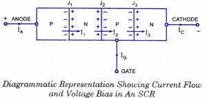
The SCR is a four-layer, three-junction and a three-terminal device and is shown in fig.a. The end P-region is the anode, the end N-region is the cathode and the inner P-region is the gate. The anode to cathode is connected in series with the load circuit. Essentially the device is a switch. Ideally it remains off (voltage blocking state), or appears to have an infinite impedance until both the anode and gate terminals have suitable positive voltages with respect to the cathode terminal. The thyristor then switches on and current flows and continues to conduct without further gate signals. Ideally the thyristor has zero impedance in conduction state. For switching off or reverting to the blocking state, there must be no gate signal and the anode current must be reduced to zero. Current can flow only in one direction.
In absence of external bias voltages, the majority carrier in each layer diffuses until there is a built-in voltage that retards further diffusion. Some majority carriers have enough energy to cross the barrier caused by the retarding electric field at each junction. These carriers then become minority carriers and can recombine with majority carriers. Minority carriers in each layer can be accelerated across each junction by the fixed field, but because of absence of external circuit in this case the sum of majority and minority carrier currents must be zero.
A voltage bias, as shown in figure, and an external circuit to carry current allow internal currents which include the following terms:
The current Ix is due to
- Majority carriers (holes) crossing junction J1
- Minority carriers crossing junction J1
- Holes injected at junction J2 diffusing through the N-region and crossing junction J1 and
- Minority carriers from junction J2 diffusing through the N-region and crossing junction J1.
Similarly I2 is due to six terms and I3 is due to four terms.
The two simple analogues to explain the basic action for the thyristor are those of the diode and the two transistor models.
- 1. Diode Model. The thyristor is similar to three diodes in series as there are three P-N junctions. Without gate bias, there is always at least one reverse biased junction to prevent conduction irrespective of the polarity of an applied voltage between anode and cathode. If the anode is made positive and the gate is also biased positively with respect to cathode, the P-layer at the gate is flooded by the electrons from the cathode and loses its identity as a P-layer. Accordingly the thyristor becomes equivalent to a conducting diode.
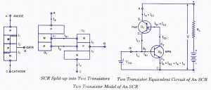
- 2. Two Transistor Model. Imagine the SCR cut along the dotted line, as shown in fig. a. Then we can have two devices, as shown in fig.b. These two devices can be recognized as two transistors. The upper left one is P-N-P transistor and the lower right N-P-N type. Further it can be recognized that the base of the P-N-P transistor is joined to the collector of the N-P-N transistor while the collector of P-N-P is joined to the base of N-P-N transistor, as illustrated in fig. c. The gate terminal is brought out from the base of the N-P-N material. This construction has been conceived merely to explain the working of SCR, otherwise in physical shape the SCR has four solid layers of P-N-P-N type only.
Now we can see that the two transistors are connected in such a manner that the collector of Q1 is connected to the base of Q2 i.e. the output collector current of Qt becomes the base current for Q2. In the similar way the collector of Q2 is joined to the base of Q1 which shows that the output collector current of Q2 is fed to Q1 as input base current. These are back to back connections of transistors in such a way that the output of one goes into as input of other transistor and vice-versa. This gives net gain of loop circuit as β1 x β2 where β1 and β2 are current gains of two transistors respectively.
When the gate current is zero or the gate terminal is open, the only current in circulation is the leakage current, which is very small in case of silicon device specially and the total current is a little higher than sum of individual leakage currents. Under these conditions P-N-P-N device is said to be in its forward blocking or high impedance ‘off state. As soon as a small amount of gate current is given to the base of transistor Q2 by applying forward bias to its base-emitter junction, it generates the collector current as β2 times the base current. This collector current of Q2 is fed as input base current to Q: which is further multiplied by β1 times as ICl which forms input base current of Q2 and undergoes further amplification. In this way both transistors feedback each other and the collector current of each goes on multiplying. This process is very quick and soon both the transistors drive each other to saturation. Now the device is said to be in.on-state. The current through the on-state SCR is controlled by external impedance only.


26 Comments
It is very important data as per the study point of view.. Thank you.
I am also very much thankful to you.
i know abt scr
Thanks fr ur information
please describe the diode model briefly.
thanks a lot.
Good stuff about scr, but i would like know about the use of gate current in more detail.
Good Explanation
Thank you
Thanks for the article given above.
scr operation is so interesting.Thanks
it’s really very good explain…
explaination is excellent
woow,really wonderfull great explanataion.. thanks a lot…..!!
it is absolutely correct, good explained article, very useful for student
its excellent very helpful to students…… thanx a lot
This is marvelous.thank you
wow,this is the time for confusion to leave me.
good explanation
I am also very much thankful to you. by your study materials
It’s very good service for both students and teachers.
It is exactly correct answer
yes i got it
Yes now i am clear about SCR. It must be useful for power electronics