TRANSFORMER-COUPLED CLASS A POWER AMPLIFIER

This is also sometimes referred to as single ended power amplifier. The term “single ended” (denoting only one transistor) is used to distinguish it from the push-pull amplifier using two transistors.
In case of a direct-coupled class A power amplifier shown, the quiescent current flows through the collector resistive load and causes large wastage of dc power in it. This dc power dissipated in the load resistor does not contribute to the useful ac output power.
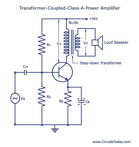
Furthermore, it is generally inadvisable to pass the dc through the output device such as in a voice coil of a loudspeaker. For these reasons an arrangement using a suitable transformer for coupling the load to the amplifier is usually employed, as shown. This arrangement also permits impedance matching.In a power amplifier circuit shown Rt and R2 provide potential divider bias ing and emitter resistor RE is meant for bias stabilization. The emitter bypass capacitor CE is meant for RE to prevent ac voltage. The input capacitor Cin couples ac signal voltage to the base of the transistor but blocks any dc from the previous stage. A step-down transformer of suitable turn ratio is provided to couple the high impedance collector circuit to low impedance load.

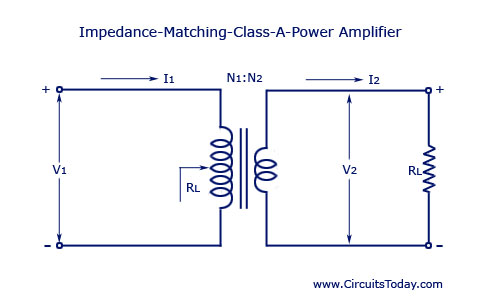
Impedance Matching. The power transferred from the power amplifier to the load (say a loudspeaker) will be maximum only if the amplifier output impedance equals the load impedance RL. This is in accordance with the maximum power transfer theorem. If we were not able to achieve the above condition, lesser power will be transferred to the load RL, though the amplifier is capable of delivering more power, and rest of power developed would be lost in the active device. Hence for transfer of maximum power from amplifier to the output device matching of amplifier output impedance with the impedance of output device is necessary. This is accomplished by using a step-down transformer of suitable turn-ratio. The transformer impedance matching circuit is shown separatel. where RL‘ is the resistance looking into the primary of the transformer and is given as
RL‘/RL = (V1/I1) ÷ (V2/I2) = V1 I2/V2 I1 = (N1/N2)2 where V1/V2 = N1/N2 and I2/I1 = N2/N1
Thus the ratio of the transformer input and output resistances varies directly as the square of the transformer turn ratio :
RL‘/ RL = (N1/N2)2 = a2 or RL‘ = a2 RL
where a is ratio of primary to secondary turns of step-down transformer, RL is the resistance of load connected across the transformer secondary and R’L is effective resistance looking into the transformer primary.

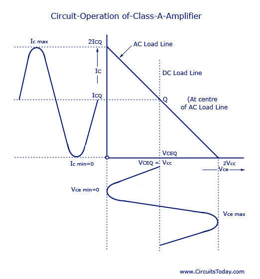
Circuit Operation. In this circuit dc (winding) resistance determines the dc load line. Typically, this resistance is quite small (assumed to be zero) providing dc load to be a vertical line rising from Vcc, as shown. When an ac signal is applied to the base of the transistor the collector current will vary around the operating point Q.
In order to have maximum ac power output, the peak value of collector current due to input ac signal alone should be equal to the zero-signal collector current. To achieve this, the operating point Q is located at the centre of the ac load line. This is achieved by adjusting the biasing circuit (R1, R2 and RE). When ac signal is applied, collector current fluctuates from maximum to minimum (zero), and operating point Q moves up and down the load line. At the peak of the positive half cycle of the input signal, the total collector current Ic max = 2 Ic and collector-emitter – voltage Vcg min = 0 while at the peak of the negative half cycle of the input signal, the collector current Ic min = 0 and collector-emitter voltage Vce max = 2 Vcc. Thus collector-emitter voltage varies in opposite phase to the collector current. The variation of collector voltage appears across primary of the transformer. Now ac voltage is induced in the transformer secondary which in turn develops ac power and supplies to the load.
Circuit Analysis. In an ideal transformer, there is no voltage drop in primary so VCEQ = VCC and power input to the transistor becomes equal to the dc power drawn from the collector supply Vcc as power loss in the primary is negligibly small. Thus power input to the transistor, Ptr = Power drawn from collector supply, Pin (dc) = VCC ICQ and overall efficiency becomes equal to collector efficiency and = Pout (ac)/ VCC ICQ
Under condition of development of maximum ac power, voltage swings from Vce max to zero and collector current from Ic max to zero. So
Vrms = 1/√2 { [Vce max – Vce min]/ 2 } = Vce max/2√2 = 2VCC/2√2 = VCC/√2
And
Irms = 1/√2 { [Ic max – Ic min]/ 2 } = Ic max/2√2 = 2ICQ/2√2 = ICQ/√2
AC power developed across the load,
Pout (ac) = Vrms Irms = (VCC ICQ)/2
Collector efficiency = Pout (ac)/ (VCC ICQ)/2 ÷ VCC ICQ = 0.5 or 50%.
Thus for a transformer-coupled class A power amplifier the maximum theoretical efficiency is 50%. In practice, the efficiency of such an amplifier is somewhat less than 50%. It is about 30%.
The efficiency of a transformer-coupled class A power amplifier can be given as
Efficiency = 50 *{ [Vce max – Vce min]/ [Vce max + Vce min]} %
The larger the value of Vce max and smaller the value of Vce min the closer the efficiency approaches the theoretical limit of 50%. Well-designed circuits can approach the limit of 50%. The larger the amount of power handled by the amplifier, the more critical the efficiency becomes!

5 Comments
mem math ka site koun sa ha1year 2nd year
what is the resistor cored
Finally i got my in4mation here so beautifuly so
thanx for that
Finally i got my in4mation here so beautifuly so thanx
wwfgh