This article teaches you how to add 32K external crystal source to AVR micro controller (Atmega8 ) with circuit diagram & C program.
Introduction
Timing-is one of the basic function, performed by the micro controllers. Every microcontroller has at least one timer/counter module in its architecture. However if the counter is clocked internally a few issues may arise in some cases. Sometimes the clock frequency may not stable, or sometimes the clock frequency may be too high than necessary. Sometimes external clock is required to have the required quality. To solve these problems, some AVR micro controllers comes up with an inbuilt oscillator supporting 32.768KHz crystal. User just need to attach the tank circuit along with the 32K Crystal.
For a demonstration of this, we would try to blink an LED. We will use the output of the timer. Microcontroller used here is ATmega8. The component list is as below:
|
Component |
Qty |
| ATmega8 |
1 |
| LED |
1 |
| Resistor |
1 |
| Push Button switch |
1 |
| 32768Hz Crystal |
1 |
| 33pF Ceramic capacitor |
2 |
| Extra: Programmer, Bread board, 5V Power Supply | |
Now, we have one Input Capture register, and we can obtain an electrical output in the OC2 Pin (PORTB, Pin 3). And we must keep the following points in mind while programming:
- Human Eye can sense any periodic activity with at least 100mS of period. TCNT2 Pre-scalar can scale down the clock frequency to ATMOST 1024th PART, Pulse Width Modulation (PWM) modes will divide the frequency to 256th part. This can give a period of AT MOST 8 Second (1024*256/32768). In this demonstration, we are pre-scaling the clock to 1024th Part.
- We can use a NON Pulse width Modulation mode like CTC mode to blink the LED too. In this demo, we are using CTC mode.
- The DDRXn bit (Data Direction Register ‘X’, Bit ‘n’) must be ‘1’, to which, the OC2 ( Output Compare of Timer/Counter 2) is connected. In case of ATmega8, it is pin no 17 of the IC. Corresponding Data Direction Register is DDRB, and pin no is 3.
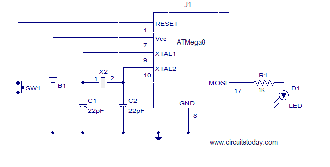
So let us make circuit and Write the program.
Fig: Circuit Diagram
// Program written for ATmega8

#define F_CPU 1000000

#include

#include

#include
void initTimr()
{ ASSR =0x08; // ASSR enables clocking
// From 32kCrystal
TCNT2 =0x00;
OCR2 =32; // As this is a CTC mode
// value of OCR2 determines
// the period
TCCR2 =0b10011111; // TCCR2 Configured for CTC mode.
// Frequency pre-scaled to
// 1024th Part.
// OCR2 toggles in compare match
while((ASSR&0x07)); // Wait until updating of the
// Above 3 register completes
TIFR =0x00;
}
int main()
{ DDRB=0b00001000; // The DDRXn bit must be ‘1’
// corresponding to OCR2
_delay_ms(2000);
initTimr();
sleep_cpu(); // Halts The CPU. Here, you
// can use ‘while(1);’ too
return 0;
}
Block: Program
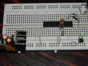
Image: Testing on Bread Board
Here is a Youtube Video of my experiment!
Asynchronous Status Register – ASSR
Asynchronous Status Register – ASSR |
||||||||
| Bit |
7 |
6 |
5 |
4 |
3 |
2 |
1 |
0 |
|
– |
– |
– |
– |
AS2 |
TCN2UB |
OCR2UB |
TCR2UB |
|
| Read/Write |
R |
R |
R |
R |
RW |
R |
R |
R |
| Initial Value |
0 |
0 |
0 |
0 |
0 |
0 |
0 |
0 |
Bit 3 – AS2: Asynchronous Timer/Counter2
When AS2 is written to zero, Timer/Counter 2 is clocked from the I/O clock, clkI/O. When AS2 is written to one, Timer/Counter 2 is clocked from a crystal Oscillator connected to the Timer Oscillator 1 (TOSC1) pin. When the value of AS2 is changed, the contents of TCNT2, OCR2, and TCCR2 might be corrupted.
Bit 2 – TCN2UB: Timer/Counter2 Update Busy
Bit 1 – OCR2UB: Output Compare Register2 Update Busy
Bit 0 – TCR2UB: Timer/Counter Control Register2 Update Busy
Significance of these bits
If a write is performed to any of the three Timer/Counter2 Registers while its update busy flag is set, the updated value might get corrupted and cause an unintentional interrupt to occur. The mechanisms for reading TCNT2, OCR2, and TCCR2 are different. When reading TCNT2, the actual timer value is read. When reading OCR2 or TCCR2, the value in the temporary storage register is read. Asynchronous Operation of Timer/Counter2 When Timer/Counter2 operates asynchronously, some considerations must be taken.
Timer/Counter Control Register – TCCR2
Timer/Counter Control Register – TCCR2 |
||||||||
| Bit |
7 |
6 |
5 |
4 |
3 |
2 |
1 |
0 |
|
FOC2 |
WGM20 |
COM21 |
COM20 |
WGM21 |
CS22 |
CS21 |
CS20 |
|
| Read/Write |
W |
RW |
RW |
RW |
RW |
RW |
RW |
RW |
| Initial Value |
0 |
0 |
0 |
0 |
0 |
0 |
0 |
0 |
Bit 7 – FOC2: Force Output Compare
Bit 6:3 – WGM21:0: Waveform Generation Mode
These bits control the counting sequence of the counter, the source for the maximum (TOP) counter value, and what type of waveform generation to be used. Modes of operation supported by the Timer/Counter unit are: Normal mode, Clear Timer on Compare Match (CTC) mode, and two types of pulse Width Modulation (PWM) modes.
Bit 5:4 – COM21:0: Compare Match Output Mode
These bits control the Output Compare Pin (OC2) behavior. If one or both of the COM21:0 bits are set, the OC2 output overrides the normal port functionality of the I/O pin it is connected to. However, note that the Data Direction Register (DDR) bit corresponding to OC2 pin must be set in order to enable the output driver. When OC2 is connected to the pin, the function of the COM21:0 bits depends on the WGM21:0 bit setting. Table 43 shows the COM21:0 bit functionality when the WGM21:0 bits are set to a normal or CTC mode (non-PWM). Table 44 shows the COM21:0 bit functionality when the WGM21:0 bits are set to fast PWM mode.
Bit 2:0 – CS22:0: Clock Select
The three clock select bits select the clock source to be used by the Timer/Counter.
Steps to configure TCNT2 in asynchronous mode
When switching between asynchronous and synchronous clocking of Timer/Counter2, the Timer Registers TCNT2, OCR2, and TCCR2 might be corrupted. A safe procedure for setting up clock source is:
- Select clock source by setting AS2 as appropriate
- Write new values to TCNT2, OCR2, and TCCR2
- To switch to asynchronous operation: Wait for TCN2UB, OCR2UB, and TCR2UB
- Clear the Timer/Counter2 Interrupt Flags
- Enable interrupts, if needed
When writing to one of the registers TCNT2, OCR2, or TCCR2, the value is transferred to a temporary register, and latched after two positive edges on TOSC1. The user should not write a new value before the contents of the temporary register have been transferred to its destination. Each of the three mentioned registers have their individual temporary register, which means that, for example, writing to TCNT2 does not disturb an OCR2 write in progress. To detect that a transfer to the destination register has taken place, the Asynchronous Status Register – ASSR has been implemented
When the asynchronous operation is selected, the 32.768kHZ Oscillator for Timer/Counter2 is always running, except in Power-down and Standby modes. After a Power-up Reset or Wake-up from Power-down or Standby mode, the user should be aware of the fact that this Oscillator might take as long as one second to stabilize. The user is advised to wait for at least one second before using Timer/Counter2 after Power-up or Wake-up from Power-down or Standby mode. The contents of all Timer/Counter2 Registers must be considered lost after a wake-up from Power-down or Standby mode due to unstable clock signal upon startup, no matter whether the Oscillator is in use or a clock signal is applied to the TOSC1 pin
During asynchronous operation, the synchronization of the Interrupt Flags for the asynchronous timer takes three processor cycles plus one timer cycle. The timer is therefore advanced by at least one before the processor can read the timer value causing the setting of the Interrupt Flag. The Output Compare Pin is changed on the timer clock and is not synchronized to the processor clock.
Pin Behavior Details
XTAL2 Pin
XTAL2: Chip clock Oscillator pin 2. Used as clock pin for crystal Oscillator or Low-frequency crystal Oscillator. When used as a clock pin, the pin cannot be used as an I/O pin. TOSC2: Timer Oscillator pin 2. Used only if internal calibrated RC Oscillator is selected as chip clock source, and the asynchronous timer is enabled by the correct setting in ASSR. When the AS2 bit in ASSR is set (one) to enable asynchronous clocking of Timer/Counter2, pin PB7 is disconnected from the port, and becomes the inverting output of the Oscillator amplifier. In this mode, a crystal Oscillator is connected to this pin, and the pin cannot be used as an I/O pin.
If XATAL2 pin is used as a clock pin, Corresponding bits from the Registers associated with the port will read 0. DDBXn, PORTXn and PINXn will all read 0; where ‘X’ is the port name, and ‘n’ is the bit.
XTAL1 Pin
XTAL1: Chip clock Oscillator pin 1. Used for all chip clock sources except internal calibrated RC Oscillator. When used as a clock pin, the pin cannot be used as an I/O pin. TOSC1: Timer Oscillator pin 1. Used only if internal calibrated RC Oscillator is selected as chip clock source, and the asynchronous timer is enabled by the correct setting in ASSR. When the AS2 bit in ASSR is set (one) to enable asynchronous clocking of Timer/Counter2, pin PB6 is disconnected from the port, and becomes the input of the inverting Oscillator amplifier. In this mode, a crystal Oscillator is connected to this pin, and the pin cannot be used as an I/O pin.
If XATAL1 pin is used as a clock pin, Corresponding bits from the Registers associated with the port will read 0. DDBXn, PORTXn and PINXn will all read 0; where ‘X’ is the port name, and ‘n’ is the bit.


4 Comments
you have left some #includes incomplete. Can you please tell which header files need to be included?
Old article I know… but for future readers, I believe the external capacitors were only required because the author did not enable the ATMega’s internal capacitors.
To use the internal capacitors for 32kHz crystal, program the CKOPT fuse and also set the appropriate CKSEL bits. See the section “Low-frequency Crystal Oscillator” in the ATMega8 data sheet.
I don’t thing you need the two bypass capacitor with low frequency.
Ahmed,
May be, actually I tried without capacitors too, But I failed. So I decided to include 22pF capacitors in the diagrams. If you refer to the Atmel’s manual upon How to use 32KHz crystals with Atmel micro controllers, they stated that it is not required to attach any capacitors. And the ccrystal should be soldered in the air with those XTAL1 and XTAL2 pins. But as I didn’t succeed practically, I would suggest everyone to stay prepared to attach 22pF caps if the set-up doesn’t work.