PIC16F877 Ports and Registers
This article is a part of our Tutorial on PIC16F877, where this section focuses on the Input/Output ports and TRIS registers of PIC16f877.
For Previous Articles, follow the links below:
TAKE A LOOK : INTRODUCTION TO PIC 16F877
TAKE A LOOK : PIC 16F877 – ARCHITECTURE AND MEMORY ORGANIZATION
TAKE A LOOK : REGISTER MEMORY ORGANIZATION IN PIC 16F877
Input/Output Ports of PIC 16F877
PIC 16F877 series normally has five input/output ports. They are used for the input/output interfacing with other devices/circuits. Most of these port pins are multiplexed for handling alternate function for peripheral features on the devices. All ports in a PIC chip are bi-directional. When the peripheral action is enabled in a pin, it may not be used as its general input/output functions. The PIC 16F877 chip basically has 5 input/output ports. The five input/output ports and its functions are given below.
- PORT A and the TRIS A Registers
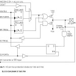
PORT A is a 6-bit wide bi-directional port, the direction of this port is controlled by TRIS Â A data direction register. Setting a TRIS A (=1) makes corresponding PORT A pin as an input, clearing the TRIS A (=0) making the corresponding PORT A pin as an output
Pin RA4 is multiplexed with the “Timer0†module clock input to become the RA4/T0CKI pin and functioning either input/output operation or Timer 0 clock functioning module. The RA4/T0CKI pin is a Schmitt Trigger input and an open-drain output. All other PORT A pins have TTL input levels and full CMOS output drivers.
Other PORT A pins in this microcontroller multiplexed with analog inputs and the analog VREF input for both the A/D converters and the comparators. The operation of each pin is selected by clearing/setting the appropriate control bits in the ADCON1 and/or CMCON registers. The TRIS A register controls the direction of the PORT pins even when they are being used as analog inputs. The user must ensure the bits in the TRISA register are maintained set when using them as analog inputs.
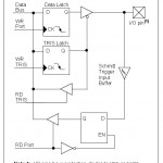
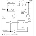
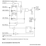
The block diagram of PORTA register is shown in the figures below.
The functions and the registers associated with PORT A register is given in the table below.
- PORT B and the TRIS B Registers
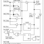
PORT B is also an 8 bit bi-directional PORT. Its direction controlled and maintained by TRIS B data direction register. Setting the TRIS B into logic ‘1’ makes the corresponding  “PORT B†pin as an input. Clearing the TRIS B bit make PORT B as an output. Three pins of PORT B are multiplexed with the In-Circuit Debugger and Low-Voltage Programming function: RB3/PGM, RB6/PGC and RB7/PGD for performing its alternate functions.
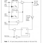
The block diagram of PORT B register is given in the figure below.
PORT B functioning table and the registers associated with PORT B is given in the table below.
- PORT C and the TRIS C Registers
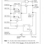
PORT C is an 8-bit wide, bidirectional PORT which controlled and maintained by TRIS C data direction register. Setting a TRIS C bit (= 1) will make the corresponding PORT C pin an input (i.e., put the corresponding output driver in a High-Impedance mode). Clearing a TRIS C bit (= 0) will make the corresponding PORT C pin an output PORT C is also multiplexed with several peripheral functions. PORT C pins have Schmitt Trigger input buffers.
When enabling peripheral functions, more care should be taken in defining TRIS bits for each PORT C pin as compared to other. Some peripherals override the TRIS bit to make a pin an output, while other peripherals override the TRIS bit to make a pin an input. Since the TRIS bit override is in effect while the peripheral is enabled, read-modify write instructions (BSF, BCF, and XORWF) with TRISC as the destination, should be avoided. The user should refer to the corresponding peripheral section for the correct TRIS bit settings.
The block diagram of PORT C register is shown in the figures below.
The functions and registers associated with PORT C register is given in the table below.
- PORT D and TRIS D Registers
PORT D is an 8-bit PORT with bi-directional nature. This port also with Schmitt Trigger input buffers, each pin in this PORT D individually configurable as either input or output. PORT D can be configured as an 8-bit wide microprocessor PORT (functioning as Parallel Slave PORT) by setting control bit, PSPMODE ((TRISE<4>). In this mode, the input buffers are TTL.
Block diagram of PORT D is shown in the figure below.
The functions and register associated with PORTD is given in table below.
- PORT E and TRIS E Registers
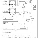
PORT E has only three pins (RE0/RD/AN5, RE1/WR/AN6 and RE2/CS/AN7) which are individually configurable as inputs or outputs. These pins controllable by using its corresponding data direction register “TRIS E”. These pins also have Schmitt Trigger input buffers. The PORT E pins become the I/O control inputs for the microprocessor PORT when bit PSPMODE is set. In this mode, the user must make certain that the TRIS E bits are set and that the pins are configured as digital inputs. Also, ensure that ADCON1 is configured for digital I/O. In this mode, the input buffers are TTL.
TRISE register which also controls the Parallel Slave PORT operation. PORT E pins are multiplexed with analog inputs. When selected for analog input, these pins will read as ‘0’s. TRIS E controls the direction of the RE pins, even when they are being used as analog inputs. The user must make sure to keep the pins configured as inputs when using them as analog inputs.
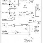
The block diagram of PORT E (in input/output mode) is shown in the figure below.
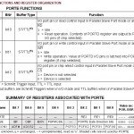
PORT E Â functions and registers associated with PORT E is given in the table below.



i am going to interface 4X4 matrix keyboard to PORTC of 16f877A with PC7-PC4 as column and PC3-PC0 as rows but portc pins C1 and C2 not responding properly
portc configured as
;——-
MOVLW 0X0F
MOVWF TRISC
;——-
SO PLEASE GUIDE ME ABOUT THIS PROBLEM
what happens to circuitstoday.com?!????? No new post 🙁 . Plese upload new posts as you can possible .
12volt 80Ah supply multiplier cct up to 150 volt Dc
load 2-3 amp need cct Diagram