We have already discussed in detail about the basics on operational amplifier, its block diagram, symbol, different characteristics, and its circuit diagram (Refer:- Op Amps-Operational Amplifiers). In this post, we will be discussing about the 741 IC, one of the most popularly used op-amp IC.
About the uA741 Op-amp IC
The 741 IC was designed by Dave Fullagar of Fairchild Semiconductor in 1968. The 741 IC is the successful predecessor of the LM 101 IC, and the only difference between the two was that an additional 30pF internal compensation capacitor was added for the 741 IC. But, this simple addition has made this IC evergreen in the electronics world and is still manufactured by different companies in different versions and specifications, and is made recognizable by adding the famous number 741 in the series.
The 741 IC is developed using the planar epitaxial process (Refer:- Epitaxial Devices – Characteristics). The IC is made ideal for use as integrator, summing amplifier, voltage follower and other basic applications.
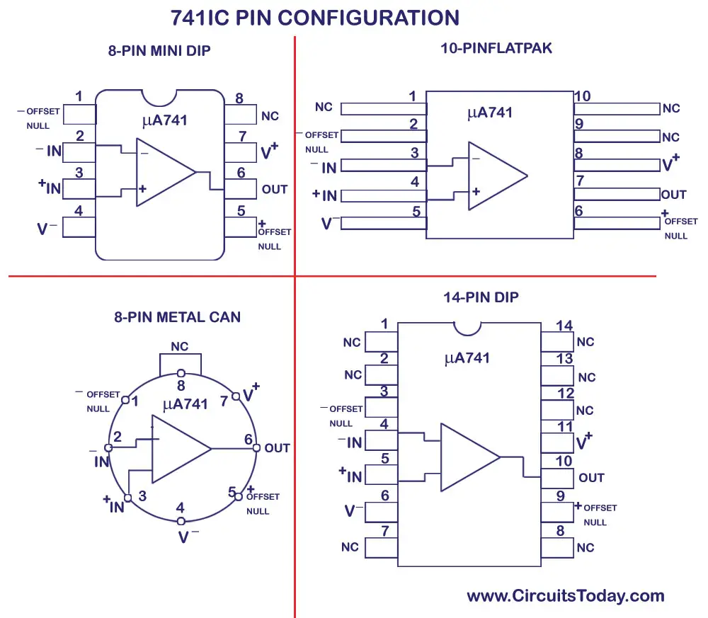
The 741 IC is available in the market as 8-pin metal can, 10-pin flat pack, 8 or 14 pin DIP. The pin configuration for thse packages are shown below.
The maximum ratings of the IC are specified for parameters like supply voltage, input and differential input voltages, storage and operating temeprature ranges, soldering pin temperatures, and output short circuit duration. The manufacturers advise not to exceed these maximum ratings even under the worst operating conditions.
The datasheet of the LM 741 IC is provided here. The equivalent circuit or schematic diagram of the 741 IC is provided in the datasheet. This equivalent circuit illustrates the internal structure of the 741 op-amp and also helps to clarify the capabilities and limitations of the op-amp. The equivalent circuit is same for all models of the 741 IC.
The electrical parameter specifications for the 741 IC is provided in 2 modes. One mode is applicable for the normal operation of the IC at room temperature of 25°C. The other mode is applicable for a commercial temperature range from 0°C to +70°C. We will be discussing all these parameters at normal temperature mode and at supply voltages of +VCC = +15V and -VEE = -15V.  It is possible to operate the 741 on a single rail supply also. This is usually done by raising the standing dc input voltage to the non-inverting input terminal to approximately half the supply voltage by a voltage divider network. The output dc voltage in such cases stands at half the supply voltage. But this does not matter because the dc can be easily blocked by a capacitor allowing only the ac signal to be passed on to the next stage.
Features of 741 IC
1. Short circuit and overload protection provided.
2. In theory, the dc output voltage will be zero if both the inputs of the 741 IC are connected to the ground. But in practice, a small dc output may appear due to minor internal unbalances. It is usually unnoticed in normal applications. But for critical conditions, the output voltage can be set precisely to zero by connecting a 10K potentiometer between terminals marked “offset-nullâ€.
3. Low power consumption.
4. Large common mode rejection ratio (CMRR) and differential voltage ranges.
5. No external frequency compensation is required. It also does not need any external compensation for phase component. This simplifies the circuit design and minimizes the number of components used.
6. No latch-up problem.
Basic Specifications of 741 IC
1. Input Offset Voltage
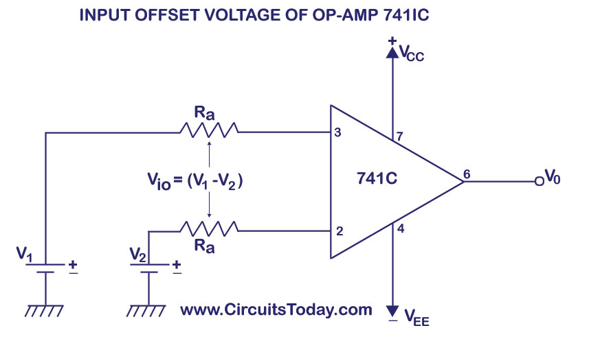
Input offset voltage is the voltage that is applied between the two input terminals of the op-amp to null the output. The figure is show below.
In the figure V1 and V2 are the input dc voltages are Ra represents the resistance applied. The input offset voltage Vio could have a positive value or a negative value. Therefore, its absolute value is listed in the datasheet. It is always better to have smaller values of input offset voltage and this indicates that the input terminal are matched better. Lowest values are 15uV for an ideal precison op-amp and the maximum value if 6mV dc.
2. Input Offset Current
Input Offset Current is the algebraic difference between the currents into the inverting and non-inverting terminals.
Input Offset Current, Iio = |Ib1 – Ib2|
Ib1 – Non-inverting input current
Ib2 – Inverting input current
The maximum input offset current value for 741 IC is 200nA. Â This value decreases as the matching between the two input terminals is improved and may reduce down to almost 6nA.
3. Input Bis Current
Input bias current is the average value of the inverting and non-inverting current.
Input Bias Current, Ib = (Ib1 + Ib2)/2
Maximum input bias current  is 500nA and minimum value is ±7nA.
4. Differential Input Resistance
Differential Input Resistance is the equivalent resistance that is measured from any one of the input terminals by keeping the other terminal connected to ground. The value for 741 IC may go as high as 2megaohms.
5. Input Capacitance
Input Capacitance is the equivalent capacitance that us measured from any one of the input terminals by keeping the other terminal connected to ground. The typical value for 741 IC is 1.4pF.
6. Offset Voltage Adjustment Range
The op-amp has pins 1 and 5 marked as offset null to determine the offset voltage adjustment range. This can be found out by connecting a 10K POT between the pin 1 (negative offset null) and pin 5 (positive offset null) and the wiper of the port should be connected to the ground. By changing the POT value, the output offset voltage can be reduced to 0V. The range through which the POT is varied to get the input offset voltage is the offset voltage adjustment range. For a 741 IC, typical value is ±15mV.
7. Input Voltage Range
The same voltage when applied to both the input terminals of the 741 IC, is called the common mode voltage and the op-amp is said to have a common mode configuration. The input voltage rage for a 741 IC is ±13V. This indicate that the common mode voltage for a 741 IC can be as high as +13V and as low as -13V without disturbing the proper working of the IC. It can also be said that the input voltage range is the range of common mode voltages over which the offset voltages apply. This method is usually carried out to know the degree of matching between the inverting and non-inverting terminals.
8. Common Mode Rejection Ratio (CMRR)
CMRR is the ratio of the differential voltage gain to the common mode voltage gain.
CMRR = Differential Voltage Gain (Ad)/ Common Mode Voltage Gain (Acm)
If the value of CMRR is high, there is better matching between the 2 input terminals. For 741IC, CMRR is 90dB.
9.Supply Voltage Rejection Ratio (SVRR)
The change in the op-amp’s offset voltage caused by variations in supply voltage is called SVRR. The change in supply voltage can be denoted by dV and the corresponsing change in input ffset voltage can be denoted by dVio.
SVRR = Change in input offset voltage (dVio) / Change in supply voltage (dV)
For 741 IC, SVRR = 150uV/V.
The lower the value of SVRR, the better will be the op-amp performance.
10. Large Signal Voltage Gain
Large signal voltage gain is the ratio between the output voltage and the voltage difference between the two input terminals.
Voltage Gain, A = Output Voltage (Vo)/ Differential output voltage (Vid)
Typical values of large signal voltage gain for 741 IC is 200,000.
11. Output Voltage Swing
The output voltage swing of the 741 IC is a 26 volt peak-to-peak undisturbed as sine wave for ac input signals (that is a value between +13V and -13V), for a load resistance value greater than or equal to 2kiloohms. This range shows the values of positive and negative saturation voltages of op-amp. The op-amp voltage swing value will not be greater than the supply voltage +VCC and -VEE
12. Output Resistance
Output Resistance is the equivalent resistance that is measured between the output terminal (Pin 6) and Ground. Typial values of output resistance of 741 IC is 75ohms.
13. Output Short Circuit Current
The op-amp has a short circuit protection built in for a certain ancient value. For 741 IC, this value is 25mA. But, for a higher current the IC will fail. Nobody would knowingly connect the output of the op-amp to the ground. But if something like that is done accidentally, the current flowing through will have a high value. This is why short circuit protection is provided. For currents higher than 25mA, external short circuit protection must be provided for 741 IC.
14. Supply Current
The supply current is the current drawn by the 741 IC from the power supply. Typical value of supply for 741 IC is 2.8mA.
15. Power Consumption
For the 741 IC to operate properly, a certain amount of quiescent power must be consumed by the op-amp. This power is called power consumption and typical value is 85mW.
16. Transient Response
Transient response is a very important factor that is used for selecting an op-amp in ac applications. Transient response along with steady state response constitutes that total response of a practical network to a given input. The response portion where a fixed value is attained right before the output is called transient response. Once reached, this fixed value remains at that level and is thus called the steady state. The steady state response does not depend on time and transient response is time invariant. Characteristics of transient response includes rise time and percent of overshoot. Transient response is inversely proportional to the unity gain bandwidth of op-amp. The bandwidth will be high when the value of rise time is low.
17. Slew Rate (SR)
Slew Rate is one of the most important parameters for selecting op-amps for high frequencies. SR is the maximum rate of change of output voltage per unit of time and is expressed in volts per microseconds.
Slew Rate, SR = dVo/dt
By calculating slew rate we can easily find out the rate in which the output of the op-amp changes in response to changes in the input frequency. The slew rate changes with change in voltage gain and is usually specified at unity gain. The slew rate of an op-amp is always fixed. Hence, if the slope requirements of the output signals are greater than the slew rate, then distortion occurs.
In the case of the 741 IC the slew rate is 0.5V/uS, which is very small. This is one reason why the 741 IC is considered not suitable for high frequency applications, such as oscillators, comparators, and filters.


nice