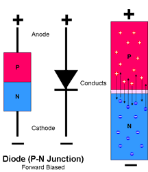
You might have read about a “Diode” in many of your text books or electronics magazines/websites. But you still don’t get the concept? Don’t worry! In this article, we explain in detail about a semiconductor diode and its properties. Well, a diode is nothing but a PN junction. We have crafted two excellent articles about PN junction before in CircuitsToday. Please read our articles “Understanding PN Junction” and then move on to read “PN Junction Characteristics“. These two articles will give you deep insights about a diode and its behavior. Now lets dig a bit about semiconductor diodes in general.
What is a diode in general?
A two electrode device is called a ‘diode‘. Its simply a P-N junction with connecting leads or terminal on the two sides of the P-N junction. Such diodes are also called a “crystal diode” because the junction is grown out of a crystal. A diode allows unidirectional flow of current and it restrains the flow in opposite direction.
- Its main advantages are cheapness,smaller size,robustness and high efficiency
- Major application is rectification which is conversion of ac to dc
A semiconductor diode can be made of either silicon or Germanium. Both differs in size and properties.
Properties of a Silicon diode:
- Smaller in size compared to Ge diodes
- Peak Inverse Voltage (PIV) is of 1000 Volts
- Silicon diodes can be operated above temperatures 200 degree celsius
- Forward voltage drop is .7 volt
- Reverse current of a Silicon diode, for a given voltage practically doubles for every 8 degree celsius rise in temperature.
Properties of Germanium Diode:
- Larger in size compared to Si diode
- PIV is of 400 volts
- Operated at temperatures in range 75 to 80 degree celsius
- Forward voltage drop is .3 volts
- Reverse current of a Ge diode doubles for every 10 degree celsius rise
Circuit and Graphical symbol of a diode:

In the figure given above, first symbol represents the circuit symbol of a semiconductor pn junction diode. The ‘P’ side of diode is always positive terminal and is designated as anode for forward bias. Other side which is negetive is designated as cathode and is the ‘N’ side of diode.
In the figure above, second symbol represents the Graphical symbol of a diode. Direction of the arrow represents the direction of conventional current flow, when the diode is forward biased.

4 Comments
it gives many information thx
i m very much satisfied from this site.
sir i want a circuit for “usb to tv9 code converter”
kindly post this circuit.