We have listed many free and paid PCB drawing software’s and simulation tools before. In this article, we are reviewing an online web based PCB schematic and simulation tool named EasyEDA. We have explained how to begin with the tool and in the process of explanation, we have shown how to draw the schematic of our popular circuit of 150 Watt Amplifier. So lets begin.
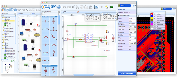
EasyEDA is a free web based EDA tool suite, integrating schematic capture, mixed-mode circuit simulation and PCB layout in a seamless on Windows/Mac/Linux web browser(Chrome, IE9+, Safari, Firefox, and Opera).This article is intended to give an overview of how to use EasyEDA to create a schematic suitable for pushing through to PCB layout, with a quick look at how it can be used to simulate circuits and a glance at the start of the PCB layout process.
Interesting? You can open http://easyeda.com/editor before reading further. Be patient, the first time to load the editor is a little bit long, but you just need one second to open it again.
Getting started
After opening the EasyEDA editor, you can find lots of components at the left hand of the canvas. The schematic used to demonstrate these steps is the Low Cost 150 Watt Amplifier Circuit. Before drawing a schematic, you are suggested to note the following tips of EasyEDA.
Tips:
- Click a component from the left panel, and then click on the canvas to place it (don’t drag because it won’t drop!)
- Right Click or Esc to go to select a mode
- Space/R keys to rotate a part, X/Y keys to flip a part. EasyEDA has many hotkeys, all of which can be configurable.
- Hold down right button and pan. It is useful for reviewing a big schematic.
- Right Click to go to select a mode, EasyEDA does not have context menu now.
Now, lets go.
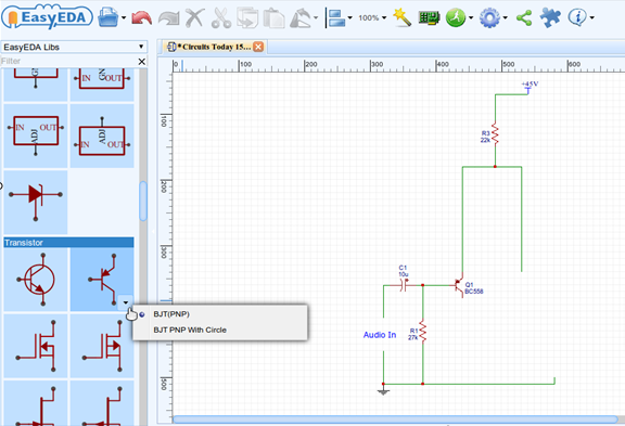
Simply clicking on a part and then clicking on the Schematic canvas places a component. Some parts have a down arrow, which when clicked, shows variants of parts that can also be placed.
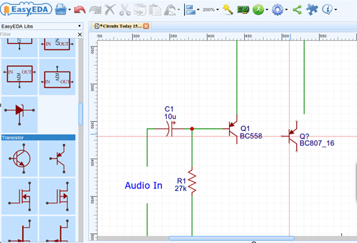
Exit component placement by right clicking. Components can then be wired up simply by clicking on the end of device pins, dragging the green wire and clicking to add corners until clicking on the destination ends the wire. The wiring mode can be invoked using the W key or from the floating Wiring Tools toolbar. Again, right clicking exits the wiring mode. Wires can be edited by selecting them and dragging the green handles around. Red dots clearly indicate that wires are joined and not just crossing.
Extensive use is made of Hotkeys in EasyEDA. A full list of these useful shortcuts can be found and edited under the blue gear Config icon at the top of the window. The Spacebar or the R key rotates and the X and Y keys flip parts whilst the device model name can be edited directly by double clicking on it or by editing it in the right hand Properties panel. Clicking back on the canvas enters the change.
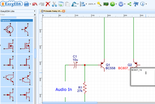
Components and wires can be dragged using the mouse or by selecting them and using the arrow keys. The effects of these are slightly different in terms of whether wires are dragged with them or not. A left to right drag selects everything fully enclosed by the box whilst a right to left drag selects everything the box intersects.
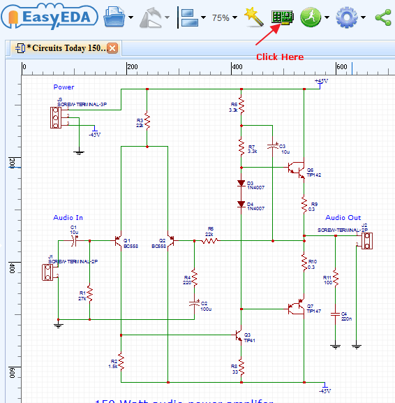
After adding input, power and speaker connectors from the SeedStudio Libs, some text (using the T key), adjusting text attributes such as size, font and colour and inserting a couple of small, linked images (by entering their urls into the Image button on the Drawing Tools floating toolbar), the completed amplifier schematic, ready to be pushed through to PCB layout with a click of the Convert Project To PCB button on the top toolbar, looks like this:
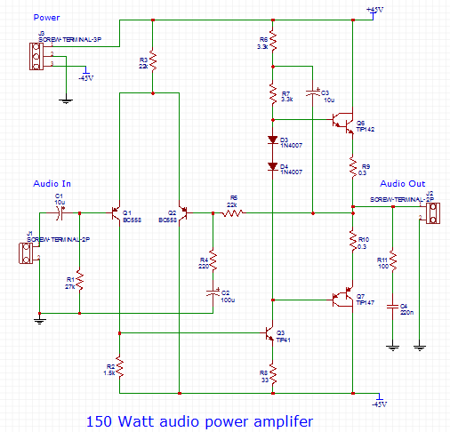
Now, This schematic is done. This schematic can be edited online, and a pdf version can be downloaded too.
Simulating the schematic
Note: simulating the Low Cost 150 Watt Amplifier Circuit is a little bit harder for newbies. If you have known nothing about Spice simulation before, you can start form EasyEDA examples first.
With a few minor modifications to add power supplies, an input signal source, a simple resistive loudspeaker load and some probes, a copy of the schematic can be made ready for a transient (time domain) or and AC Analysis (Bode plot) simulation:
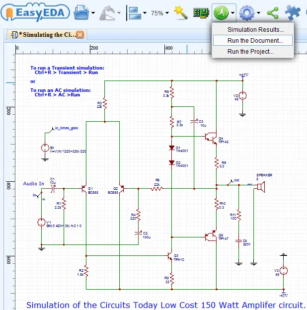
.
Clicking on the Green Man icon and selecting Run the Document… or simply typing Ctrl+R opens the simulation dialogue box and from there the type of simulation and the relevant simulation parameters can be set and then run by clicking on the Run key.
Depending on the type of simulation that is run, the results and any error messages are shown in text form in the Simulation Results –> Show your simulation report window or in plot form in the powerful WaveForm viewer. A spice netlist of the simulation can be downloaded from the Show your simulation report window and plots in the WaveForm viewer can be analysed using the on-screen cursors.
The display area, trace, grid and background colours and the placing and hiding of traces on up to 3 grids in WaveForm can all be easily tailored from the WaveForm Config button.
WaveForm plots can also be saved into Project folders where they can be re-opened and manipulated the same as when they are first generated. Saved WaveForm plots can be exported in a .pdf, .png and .svg formats.
So, for example:
Ctrl+R > Transient > Run
generates a time domain WaveForm plot:
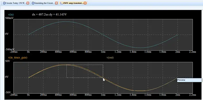
and:
Ctrl+R > AC Analysis > Run
generates a frequency response WaveForm plot:
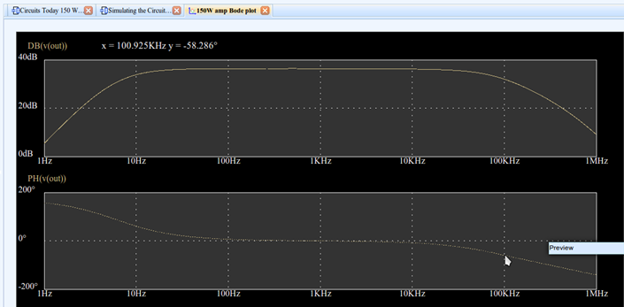
Pushing the schematic through to PCB design.
Going back to the “passive” or non-simulation schematic and clicking on the Convert Project To PCB button opens the Verify the packages dialogue where any last minute changes and corrections can be made:
Clicking Build PCB then opens the PCB design canvas with a default board area and all the components set to one side, connected by ratlines ready.
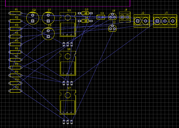
Next, a couple of hours need to cost for making this audio project done.
Account Management
EasyEDA is a web-based service and although you are free to use it in anonymous mode which you can do without creating an account, you are much better off creating an account to manage your own designs and parts libraries. Creating an account is easy and gives you free access to the full power of EasyEDA for as long as you wish.
Click on Join – given on the the user menu:
After clicking on Join, a very simple Create an account dialog opens.
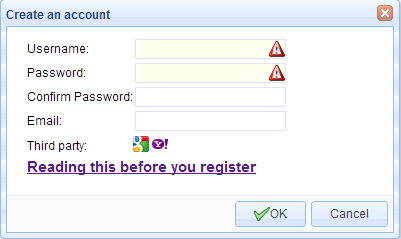
If you have a Google or Yahoo account, you can click the third party icons directly to create an account.
Final Notes
It is difficult to do justice to such a flexible and comprehensive tool in just a few pages and screenshots. There are many powerful functions such as symbol and footprint creation and editing, basic hierarchy, adding models and subcircuits to spice symbols and schematics, collaborative designing that have been left out.
More in-depth information can be found in the EasyEDA Tutorial but it is hoped that this article has at least given the you a quick start guide in how to drive EasyEDA and a flavour of the many features it provides to make an Easier EDA Experience.



8 Comments
hi sir how can we make powerful this one for examle 500wat
Nice sharing, It is awesome. I think EasyEDA is the just software which I try to find .
one new mini project ckt my mail id send sir
Draw schematic online, genius idea, great tool.
this is best sofware i have ever seen,u can simulate ur circuits at any places it just required net connection. i thank to that person who made such a useful sofware.
This is the best software that I used to draw a circuit. It didn’t take long to learn and design a board. I can’t wait to order some PCBs to test out.
Thanks.
This simulation software is so much helpful for us.
You need 4 diodes to prevent cross-over distortion