Programmable UJT (PUT).
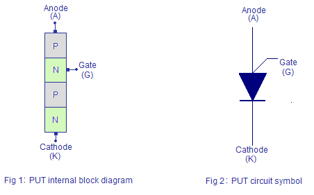
Programmable unijunction transistor or PUT is a close relative of the thyristor family. Its has a four layered construction just like the thyristors and have three terminals named anode(A), cathode(K) and gate(G) again like the thyristors. Yet some authors call it a programmable UJT just because its characteristics and parameters have much similarity to that of the unijunction transistor. It is called programmable because the parameters like intrinsic standoff ratio (η), peak voltage(Vp) etc can be programmed with the help of two external resistors. In a UJT, the parameters like Vp, η etc are fixed and we cannot change it. The main application of programmable UJT are relaxation oscillators , thyristor firing, pulse circuits and timing circuits. ON Semiconductor® is the only manufacturer of PUT now. 2N6027 is the most common type number and it is available in the TO-92 plastic package. The internal block diagram and circuit symbol of PUT are shown below.
From the above figure, you can see that the PUT has a four layered construction. Topmost P-layer is called the anode (A). The N-layer next to the anode is called the gate (G). The P-layer next to the gate is left alone. The bottom most N-layer is called cathode (K). Ohmic contacts are made on the anode, cathode and gate layers for external connection.
PUT characteristics.
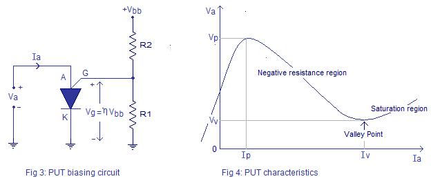
PUT characteristics is essentially a plot between the anode voltage Va and anode current Ia of the PUT. The typical biasing diagram and characteristics plot of a PUT is shown below.  Typically the anode of the PUT is connected to a positive voltage and the cathode is connected to the ground. The gate is connected to the junction of the two external resistor R1 and R2 which forms a voltage divider network. It is the value of these two resistors that determines the intrinsic standoff ratio(η) and peak voltage (Vp) of the PUT.
When the anode to cathode voltage (Va)is increased the anode current will also get increased and the junction behaves like a typical P-N junction. But the Va cannot be increased beyond a particular point. At this point sufficient number of charges are injected and the junction starts to saturate. Beyond this point the anode current (Ia) increases and the anode voltage (Va) decreases. This is equal to a negative resistance scenario and this negative resistance region in the PUT characteristic is used in relaxation oscillators. When the anode voltage (Va) is reduced to a particular level called “Valley Point”, the device becomes fully saturated and no more decrease in Va is possible. There after the device behaves like a fully saturated P-N junction.
Peak voltage (Vp): It is the anode to cathode voltage after which the PUT jumps into the negative resistance region. The peak voltage Vp will be usually one diode drop (0.7V) plus the gate to cathode voltage (Vg). Peak voltage can be expressed using the equation:
Vp = 0.7V + Vg = 0.7V + VR1 = 0.7V + ηVbb . Where η is the intrinsic standoff ratio and Vbb is the total voltage across the external resistor network.
Intrinsic standoff ratio ( η) : Intrinsic standoff ratio of a PUT is the ratio of the external resistor R1 to the sum of R1 and R2. It helps us to predict how much voltage will be dropped across the gate and cathode for a given Vbb. The intrinsic standoff ratio can be expressed using the equation:
η = R1/(R1+R2).
PUT relaxation oscillator.
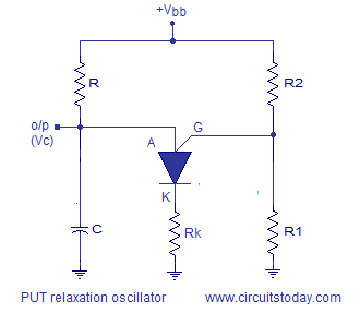
Relaxation oscillator is of course the most common application of a programmable UJT. PUT relaxation oscillator can be used for generating a wide range of saw tooth wave forms. It is called a relaxation oscillator because the timing interval is started by the gradual charging of a capacitor and the timing interval is terminated by the sudden discharge of the same capacitor. The circuit diagram of a PUT relaxation oscillator is shown below.
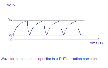
 Resistors R1 and R2 set the peak voltage (Vp) and intrinsic standoff ratio (η) of the PUT. Resistor Rk limits cathode current of the PUT. Resistor R and capacitor C sets the frequency of the oscillator. When the supply voltage Vbb is applied, the capacitor C starts charging through resistor R. When the voltage across the capacitor exceeds the peak voltage (Vp) the PUT goes into negative resistance mode and this creates a low resistance path from anode(A) to cathode(K). The capacitor discharges through this path. When the voltage across the capacitor is below valley point voltage (Vv) the PUT reverts to its initial condition and there will be no more discharge path for the capacitor. The capacitor starts to charge again and the cycle is repeated. This series of charging and discharging results in a sawtooth waveform across the capacitor as shown in the figure below.
 The frequency of oscillation of a PUT relaxation oscillator can be expressed by the following equation:
F = 1/ (RC ln(1/(1-η)).Where F is the frequency, η is the intrinsic standoff ratio, R is the resistance and C is the capacitance.
PUT relaxation oscillator testing.
Added soon.


8 Comments
Please share a SCR triggering circuit with detailed component values.
Really helpful information. It helps me a lot
thank this note really helping me in my assiment..
very easy